
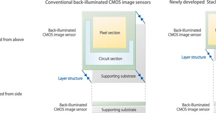
Sony Semiconductor Solutions Corporation (“Sony”) has succeeded in developing the world’s first*1 stacked CMOS image sensor technology with 2-Layer Transistor Pixel. Whereas conventional CMOS image sensors’ photodiodes and pixel transistors occupy the same substrate, Sony’s new technology separates photodiodes and pixel transistors on different substrate layers. This new architecture approximately doubles*2 saturationContinue Reading

IntroductionThere is a clear trend and market need for high-power transmission over cable. Power over HDBaseT (POH) enablesthe transfer of DC power in conjunction with data signals over a single Ethernet cable to a distance of up to 100meters (m). The POH standard is based on the IEEE 802.3at standardContinue Reading

 Last month we posted a blog about HDBaseT that explained the application and how testing isn’t really any different since standards-based Category 5e, 5 or 6A will support it. But maybe you’ve also heard about power over HDBaseT, or POH, and you’re wondering how that differs from power over Ethernet (PoE). AContinue Reading

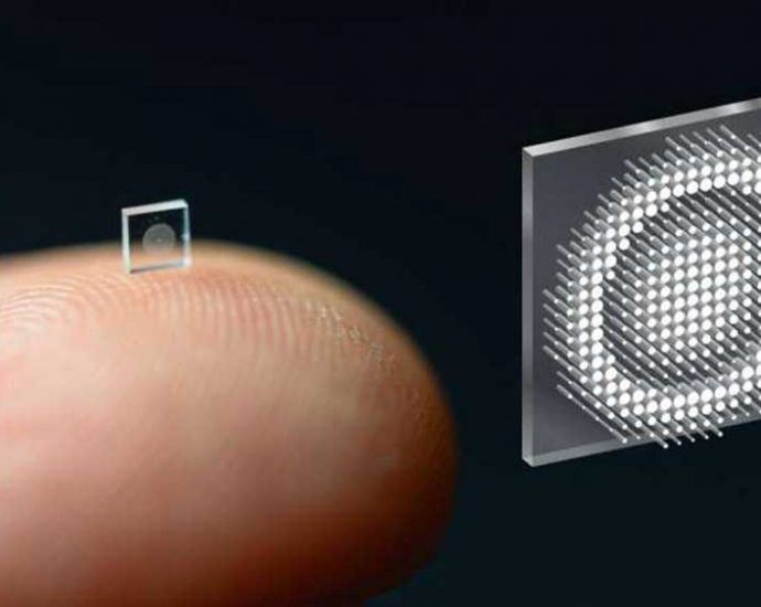
by Molly Sharlach, Princeton University Micro-sized cameras have great potential to spot problems in the human body and enable sensing for super-small robots, but past approaches captured fuzzy, distorted images with limited fields of view. Now, researchers at Princeton University and the University of Washington have overcome these obstacles with anContinue Reading

By: Ángel Díaz In every age, police forces gain access to new tools and technologies that may advance their mission to prevent and combat crime. The deployment of new technologies requires an understanding of their impacts on the fundamental rights of the communities that police serve and the development ofContinue Reading

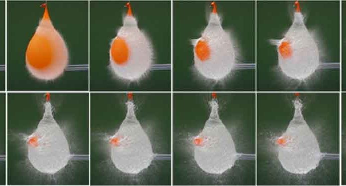
Faster than the Human Eye! Higher Speed with Column-parallel A/D Conversion and Reducing Noise The key to increased speed of Sony’s CMOS Image Sensor can be found in parallel signal processing. CMOS sensors have analog-digital (A/D) conversion circuits that convert analog pixel signals into digital signals (Figure 1). Speed isContinue Reading

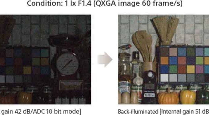
Greater Sensitivity than the Human Eye! Back-illuminated structure provides higher sensitivity Sony’s back-illuminated CMOS image sensor improves sensitivity and noise reduction – the key factors to enhancing image quality, while radically realigning their fundamental pixel structure from front-illumination to back-illumination. It has retained the advantages of CMOS image sensors suchContinue Reading

Adding Functional Value to a CMOS Image Sensor that Exceeds Human Vision! Back-illuminated and stacked structure provide advanced functionality Stacked CMOS Image Sensor is a Sony’s CMOS image sensor that adopts a unique ‘stacked structure.’ This structure layers the pixel section, containing formations of back-illuminated pixels over the chip affixedContinue Reading

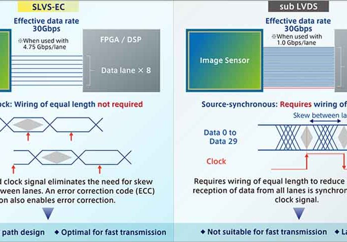
What’s SLVS-EC? Scalable Low-Voltage Signaling with Embedded Clock, abbreviated SLVS-EC, is a high-speed interface standard developed by Sony for fast, high-resolution image sensors. The interface’s simple protocol makes it easy to build camera systems. Featuring an embedded clock signal, it is a good choice for higher speeds or transmission overContinue Reading